Browse Resources
Resources | |
|---|---|
This video, provided by the Nebraska Nanoscale Facility (NNF), offers a tour of a photolithography room. Photolithography, also known as optical lithography or UV lithography is "a process used in microfabrication to pattern parts of a thin film or the bulk of a substrate," using "light to transfer...
This webinar, hosted by ATE Central, provides information about intracortical neural interfaces (INI). In particular, the webinar "focus[es] on studies of silicon carbide (SiC) micromachined semiconductor neural devices and the materials challenges that must be understood and overcome to bring this...
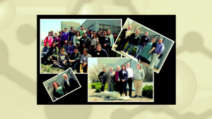
This video, created by the Center for Nanotechnology Education (Nano-Link), provides an overview of the Ninth Annual Nano-Link Conference. Students are shown talking about their experiences, learning about nanoscience topics in laboratory environments, playing Nano-Link Jeopardy, giving poster...
This document, provided by NUE: Exposing Engineering Students to Nanoscience and Nanotechnology at the University of North Dakota, is an article describing the work of four faculty members from the University of North Dakota to establish a nanoscience and nanotechnology program at their institution....
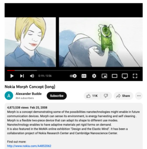
This video clip covers technology advancements being developed by Nokia. These include electronics materials and films that can be stretched or folded to wear as a bracelet on your arm, used to sense different types of contamination in the air or on fruit, touch key pads that go from being flat on...
This lesson, presented by the National Nanotechnology Infrastructure Network, covers the general concepts of measurement by using a pool noodle to measure objects. The activity "encourages students to consider features that are useful when developing or using a measurement tool." The lesson...
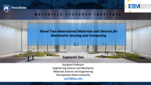
This webinar, provided by the Nanotechnology Applications and Career Knowledge Support Center (NACK Center), discusses two dimensional materials and advances in using them for sensing and computing. The webinar is presented by Dr. Saptarshi Das, Assistant Professor of Engineering Science and...
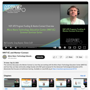
This video from the Micro Nano Technology Education Center (MNT-EC) is part of a series of seminars on micro nano technologies and issues in the field. In this video, Mel Cossette, Elaine Craft, and Greg Kepner describe what Mentor-Connect is and how the MNT-EC can mentor participants in writing...
This video from the Indian Institute of Technology is a lecture that demonstrates ohmic contacts on semiconductors. The lecture includes slides with equations illustrating related concepts. This video runs 57:48 minutes in length.
This paper, from Adam Filios, Yeong S. Ryu, and Kamal Shahrabi, of Farmingdale State College, covers optical properties and application of nanoscale silicon. Topics covered include the importance of silicon, silicon optoelectronics and nanotechnology, light emissions from nanoscale silicon, and...
| |
| ← Previous | Next → |
